Research & Development (8)

R&D Vision, Mission and Strategic Objectives

Vision

CARSEM CTC to be recognized as the preferred partner for semiconductor subcontracting & the ideal place to work for the best engineering talent in this region.

Mission

To explore new frontiers, develop technologies & competencies in line with customer needs that would provide CARSEM a competitive edge in increasing revenue & profitability.

Strategic Objectives

  • To ensure that Carsem’s technology roadmap aligns with or is as close as possible to our key customers
  • To minimize time to market through efficient process, planning & resourcing of R&D Projects
  • To keep customers updated on R&D progress while ensuring that we extract maximum commercial value from our R&D programs
  • To identify packages and technology opportunities that are new & innovative, and may not be on Carsem’s existing roadmap
Strong & Experienced Team

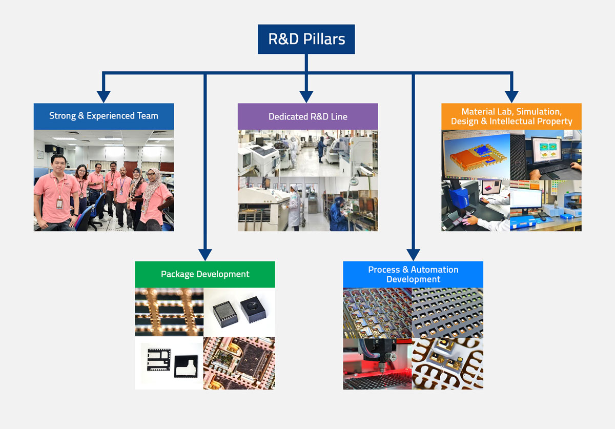
Our team is composed of people from various backgrounds and strong industry expertise. We have expertise in material development that includes mechanical, thermal and electrical testing lab, along with simulation & design team – one of the core strengths in package development. In order to ensure the success of high volume manufacturing, we have the package development team as well as the process & automation development team that function together coherently.

These people are the ones running various experimental designs in our dedicated R&D line, aiming to perfect the processes & product outcomes. Furthermore, our team has full capability to run reliability testing to ensure the robustness of the products that are assembled and manufactured. Last but not the least, we have the intellectual property team to compile our innovative technology and to ensure that the technology we venture in is novel and protected.

Dedicated R&D Line

Our dedicated R&D Line is well equipped to formulate and implement strategies for new packages, assembly process technology, and materials to enhance manufacturing capability.

The R&D Line is a dedicated floor space occupied by equipments covering the front of line and the end of line. In this line, we run production for packaging, process and material development.

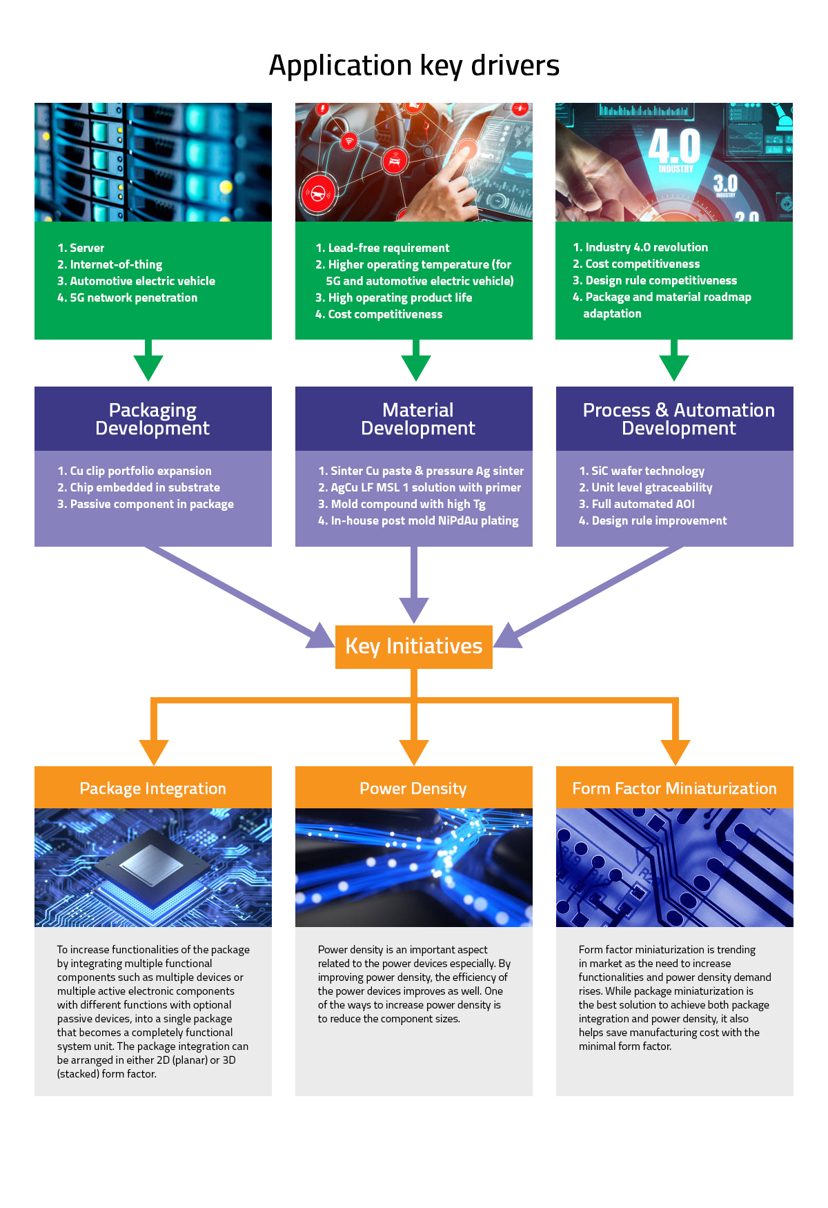
Some of the projects driven via the pilot line include engineering and qualification for the development of copper clip, flip chip, cavity package, and other type of packages mainly for the automotive customers. There’re also material development projects run on the R&D line such as copper sinter paste, AgCu lead frame MSL 1 solution with primer, and high thermal properties for mold compound.

Material Lab, Simulation, Design & Intellectual Property

The material lab comprises of various testing equipments for mechanical, thermal, and electrical properties. Situated in our R&D line, the labs are easy to access by our team members and have become solution provider for our R&D projects. The material lab also provides reliability testing such as MSL, CSAM, xSection, Reflow, etc. We have thermal and electrical simulation testing as well as lead frame design capability. The intellectual property team works along with the legal team to review and study the technology.

Novelty of an innovative  technology drives our company to protect the technology in terms of patent publications, contributing to the technology development in the world of electronics. While most of our patents are filed in Malaysia, United States and China, some are also filed in Europe and other Asian countries. Our patents are spread across several innovative technologies related to semiconductor packaging, processes and materials, such as package integration, power density, and form factor miniaturization. We firmly believe that these technology advancements enable us to support our customers’ transformation innovations, and are aligned with the Industry 4.0 requirements. Currently, Carsem owns a total of 75 active patents.

Process & Automation Development

Modern technological advances drive the development of process and automation in Carsem. With the current needs of high power applications, automated inspection and data tracking, we have been running development with various designs of experiment and qualifications in order to ensure a smooth running process. Our R&D group has become a pioneer in several process & automation technologies such as Unit Level Traceability with the 2D dot matrix marking, and also in 3D automated vision inspection for Flip Chip devices.

Package Development

CTC has been developing a wide range of packages for the electronics industry applications – ranging from the telecommunication, automotive to the power market. We are attentive towards our customers’ ever evolving requirements, and strive to develop robust packaging that suits their needs without compromising the quality of the products. With ‘state-of-the-art’ equipments in our dedicated R&D line, we are able to provide the best quality custom packaging solutions to our customers.

Key ongoing R&D initiatives